

Design modifications
(Getting technical now, read ahead first if you want to see how the circuit works).
Surprisingly, I have not read about this problem elsewhere, even though it is an obvious and understandable issue with such diode based envelope circuits. Even more surprising, my Microbrute does not show this issue, although it almost certainly has the same envelope circuit (the Minibrute, at least, has the exact same ADSR). Well, anyway, I decided to fix it and my final solution was to use a type of precision rectifier in place of the decay and release diodes (hence the title). It's a bit of a special one, because it rectifies current in stead of voltage. The basic schematic is as follows:

The opamp's negative input is a virtual ground point. For a positive input voltage, a current flows through the resistor as defined by Ohm's law. This current flows through the diode into the opamp output. The output therefore is at a negative voltage, which compensates the diode's forward voltage drop. For a negative input voltage, however, the diode cannot conduct any current (the opamp will saturate at the positive rail). So, this circuit can sink a current, but not source any.
Complete circuit
Here is the complete circuit of my implementation:

All transistors are BC547C (but can probably be almost any NPN), all diodes are 1N4148 (apart from L1, which is a red LED). U1 is an Intersil ICM7555, and U2 is a TL074 quad opamp (powered from +12 V and -12 V). The maximum current draw is about 10 mA from both the positive and the negative rail. C6 should be close to U2 on the board.
Gate input
The first part of the circuit converts an incoming gate signal or button press into a well-defined gate signal (GATE) and a short trigger pulse (TRIG). Q1 and Q2 form a discrete Schmitt trigger, turning any input signal into a gate with sharp edges between 0V and 12V. C1 and R6 turn the sharp edge into a short pulse of a few 10s of microseconds, which is then buffered and inverted by Q3. So the TRIG signal is normally at 12V and makes a short pulse to 0V at the start of each GATE.
7555 timer core
These signals are used to start the 7555 timer via the trigger and reset pins (these are both inverting inputs - e.g. a high input on pin 4 means not reset). The Out pin will go high (to 12V), and the Discharge pin will be floating. The timing capacitor C3 will start charging from Out thourgh D2 and the Attack potentiometer. The voltage over C3 is buffered by U2c, giving the envelope output.
The buffered output is also fed back to the 7555s Threshold pin. When this pin reaches 2/3 VDD (about 8V), the timer will switch off. Out will go low, so the charging will stop. At the same time the Discharge pin is connected to ground. R14 now defines a sustain voltage between 0 and 8V, and the precision rectifier of U2b/D4 allows C3 to discharge through the Decay pot to the sustain level.
The output will remain at the sustain level until the gate signal ends. When GATE goes to 0V, the U2a/D3 rectifier allows discharge through the Release pot until finally reaching 0V output.
Inverted output and LED driver
Yusynth uses one additional opamp to invert the output, and one as a LED current driver, but I had only one opamp left. While the inverted output is not essential, I found these functions can be combined, which is done in U2d. This is again similar to a precision rectifier. R17 converts the envelope voltage to a current, which is then (for positive input) forced to go through the LED. Again, the opamp compensates for the LED forward voltage drop. The current also goes through R19, which gives the inverting amplifier function. This voltage is tapped of as second output. D6 is there such that the opamp never goes to the positive rail, which would be too much reverse voltage for a typical LED.
Built circuit
Breadboard version:

Version built on prototype board:
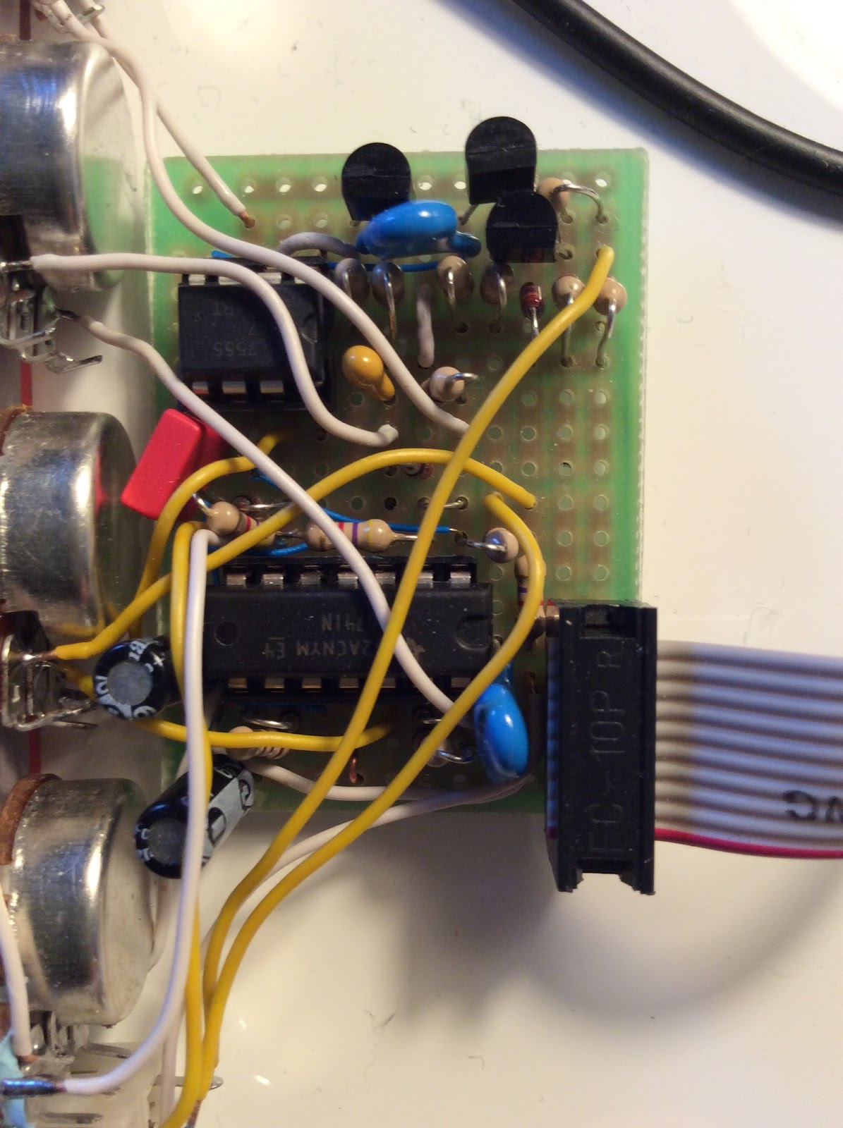
I used a piece of board designed for DIP packages, which turns out to work quite well for the discrete transistor stages as well. Most resistors and diodes are on their side to make it fit, and a bunch of jumper wires and solder bridges complete the connections. This is probably not the style for everybody, as the result is always chaotic, but it gives quite compact results for a prototype board (much more than the typical veroboard layout). The board is held in place only by the connecting wires. The front panel is a prototype cut out of cardboard (4HP eurorack size).

Finally a picture of the back. Note the generous use of solder. The three small wire bridges were needed because I accidentally inverted all the power lines when planning the board...
Performance
I'm quite satisfied with the result. The decay and release phases go nicely to their final level (sustain or 0 V, respectively) without any slowing down. A nice side effect is that the reverse leakage through the decay diode (which is now bigger because the opamp can create a large reverse voltage) compensates leakage of the timing capacitor and through other diodes, so the sustain phase stays accurate indefinitely. After the final release there is an output offset on the order of 10 mV (presumably the low voltage of the gate and discharge signals), but this is quite acceptable and it seems stable.
 |
| ADSR envelope |
 |
| Shortest AD envelope |
Further modifications
- Analog Output has further evolved this design by adding retrigger and loop functions. See his blog post and this youtube video with detailed explanations. He also shares the PCB design in Kosmo format.